
 English
 Japanese

Samsung Breaks Barriers to 7nm LPP Node Technology
The Road to EUV Technology
Since 2000, Samsung has been doing research and development in EUV. The company has made outstanding progress in this area through collaborative partnerships with industry-leading tool providers to design and install completely new equipment in its manufacturing facilities to ensure the stability of EUV wafers. The initial EUV production started in Samsung's S3 Fab in Hwaseong, Korea.
By 2020, Samsung expects to secure additional capacity with a new EUV line for customers who need high-volume manufacturing for next-generation chip designs. As an EUV pioneer, Samsung has also developed proprietary capabilities, such as a unique mask inspection tool that performs early defect detection in EUV masks, allowing those defects to be eliminated early in the manufacturing cycle.
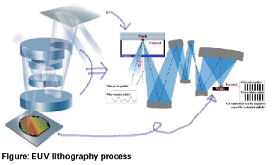
"Commercialization of EUV technology is a revolution for the semiconductor industry and will have a huge impact on our everyday lives," said Peter Jenkins, Vice President of Corporate Marketing at ASML. "It is our great pleasure to collaborate with Samsung and other leading chip makers on this fundamental shift in semiconductor process manufacturing."
7nm LPP EUV Ecosystem
The Samsung Advanced Foundry Ecosystem (SAFE) is also fully prepared for the introduction of 7LPP with EUV. Ecosystem partners across the industry will be providing foundation and advanced IP, advanced packaging, and services to fully enable Samsung customers to develop their products on this new platform. From high-performance and high-density standard cells to HBM2/2e memory interfaces and 112G SerDes interfaces, SAFE is ready to help customers implement their designs on 7LPP.
Issues at Hand
Yet, many challenges still remain unsolved as EUV equipment and tools are intrinsically ultra-high powered and needing ultra-high temperature, thus requiring ultra-high electricity power to generate EUV light. The rugged and rigid working environments have been calling for dramatic changes in the peripheral tools and components, like photomasks, pellicles, and photoresist. For example, pellicles are required to be more resistant to high temperatures and high source power of 250W and 320W, while keeping transparency rate above 90 percent. Photoresist materials are also required to be more sensitive to light.
Improving productivity also proves to be a daunting task. Today, first-generation EUV scanner can process 125 wafers per hour. ASML has a roadmap to improve the low productivity in 2019 and beyond, going through technology evolutions from a second- to third-generation to high numerical aperture EUV. Its ultimate goal is to process 185 wafers per hour by 2022 at a source power of 250W.