
 English
 Japanese

Data-Driven Apps Offer Opportunities, Hurdle Challenges
As with the case, semiconductor chip sales peaked in 2017 at an all-time high of US$400 billion, a 20 percent year-on-year jump, mainly driven by explosive demand for memory chips, like DRAM and NAND flash memory chips, of which sales grew by 74 percent and 44 percent, respectively.
In 2018, shipments of semiconductor chips will grow 6 percent to 8 percent to hit US$450 billion, as high-performance computing, IoT and automotive applications will keep driving demand.
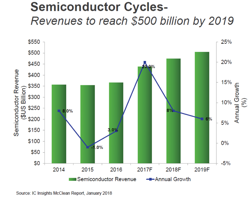
Fig. 1: Semiconductor cycles
Challenges of Finer Circuitry
Yet, it will not be easy to keep up with the growth momentum, as upcoming technology challenges are getting increasingly tough to tackle. The most daunting challenge is how to scale down the fine pitch of chip patterns below 10nm circuitry without compromising yield.
"In the past, scaling down the chip circuitry not only allowed chip makers to cram more transistors in a given space to improve chip performances, but also to cut costs and power consumption and boost productivity. When it comes to 10nm and below circuitry lithography, however, costs tend to go up, as it is increasingly getting tough to detect defects. That is because the smaller the chip circuitry pattern gets, the smaller the impurity defect particles, thus doing harm to yields," stressed Kang.
To tackle that issue, chip makers are now cooperating with materials providers to find a way to filter out microscopic impurity particles in advance.
"As the chip circuitry gets down below 7nm wide, it is almost impossible to see and inspect whether the patterns are etched properly using today's optic light-source-based inspection equipment. The only way available is to filter out or crystallize and purify materials like gases and chemicals," says Richard Hong, President of Entegris Korea, a Korean subsidiary of U.S.-based Entegris.
Entegris is a total solutions provider that supplies materials, likes gas and chemicals, gas carrier canisters, and other filters and purifiers.
Equally important is to perfectly control material contamination from production all the way through delivery, storage, and carrying to clean rooms. Indeed, this is the time when materials innovation and physics matter more than chip pattern lithography technology in improving yield and chip performances