
 English
 Japanese

Data-Driven Apps Offer Opportunities, Hurdle Challenges
Take 3D NAND flash memory chips for example, which help greatly boost up storage density in a given space by stacking up cells in three dimensions, thus paving the way for solid state drive (SSD) markets. To stack layers over layer of cells as high as 100, chip makers have to etch holes as thin as 1/500 that of human hair 100 layers deep on silicon wafer all at once. Otherwise, it would compromise such tall structures.
To tackle that issue, Samsung is working to commercialize a new breed of cryogenic etching methodology, which uses cryogenic physics to dig holes as deep as more than 100 layers all at once at -30°C without compromising hole structures.
Kang said that it would take years to commercialize the cryogenic etching technology.
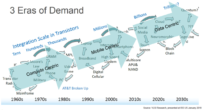
Fig. 2: Three eras of semiconductor demand
Samsung's years-long work on magnetic RAM is another example of how the chip maker have been struggling to innovate itself on physics and material technology. To develop magnetic RAM, Samsung has adopted a new breed of etching materials called ion-beam etchants as well as new physics called atomic layer etcher. Samsung is scheduled to start mass production of magnetic RAM in 2019, as these two technologies are to be soon put to commercial use.
Samsung has been also working together with material makers to find new photoresist materials, which are thick enough to draw circuitry lines as high as six to nine layers all at once.
As it is costlier and time consuming to stack layer one by one, Samsung has been heightening the thickness of photoresist materials by 30 percent when it comes with a new generation, according to Kang.
The commercialization of HBM or high-bandwidth memory technology requires new packaging materials like film types. HBM is a high-performing RAM interface technology that vertically strings together up to eight DRAMs one on top of the other using through silicon via hole and micro-bumps.
Critical to the HBM interface packaging is how to fill in thin gaps between each DRAM chip, which is as thin as several nanometers. Samsung and materials makers are working together to develop a method that thermalize thin films to fill in the gap.
"Over the past decades, PCs gave way to Internet as a prime growth driver for semiconductor chip market in early 2000s, and then smartphones displaced the Internet connectivity as a main growth engine in late 2010s. Today, AI and big data analytics are taking the place to drive demand. Yet, all players in the ecosystem have to cooperate to innovate themselves on equipment, materials, and utility infrastructures to keep the growth momentum up and running," stressed Kang.