
 English
 Japanese

Advance PWBs Gain Traction in New Growth Fields
As automobiles become highly computerized, the number of electronic control units (ECUs) incorporated in a vehicle has been increasing. They require PWBs with excellent heat resistance, as their installation environment has shifted from a cabin to an engine compartment, and then to direct-mounting on an engine. In addition, meeting the requirement for smaller PWBs, the downscaling of pattern specification is expected to advance from the existing line/space (L/S) widths of 130μm/170μm to L/S of 100μm /100μm, and furthermore to L/S of 75μm/75μm.
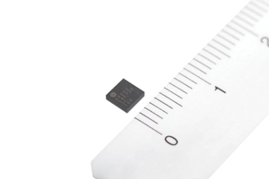
Photo 3: A Bluetooth Low Energy module measuring 3.5×3.5mm,
which uses component-embedded PWB (TDK Corporation)
Finer PWBs for Smartphones, Modules
The use of highly reliable any-layer PWBs that employ all-layer laser vias and filled plating for main boards of smartphones has become widespread as well. Microfabrication technologies with L/S of 50μm/50μm and smaller are applied for any-layer PWBs. The via diameter of laser vias has been reduced to 75μm or smaller. In addition, substrate thickness of around 0.3mm for six-layer PWBs has been achieved.
For the purpose of achieving smaller modules with higher functions, component-embedded PWB technologies have come to be employed.
The thicknesses of components to be embedded have also been reduced to 0.11mm for multilayer ceramic capacitors (MLCCs) and 0.14mm for resistors. As a result, the miniaturization of various high-functional modules has been achieved.