
 English
 Japanese

Samsung Breaks Barriers to 7nm LPP Node Technology
S
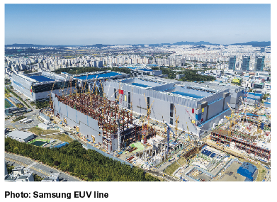
amsung Electronics Co., Ltd. has started wafer production of a 7nm node low power plus (LPP) process technology using extreme ultraviolet (EUV) lithography technology.
The actual production of the 7LPP node is a clear testimony to Samsung's successful adoption of EUV technology, paving the road map to 3nm node.
The successful migration to 7LPP has a wide range of ramifications, as it enables Samsung and its foundry partners to innovate on its chip architecture to meet the system requirements of 5G mobile communications ecosystems, including artificial intelligence, enterprise and hyperscale datacenter, IoT, automotive, and networking.
"With the introduction of its EUV process node, Samsung has led a quiet revolution in the semiconductor industry," said Charlie Bae, Executive Vice President of Foundry Sales and Marketing Team at Samsung Electronics. "This fundamental shift in how wafers are manufactured gives our customers the opportunity to significantly improve their products' time-to-market with superior throughput, reduced layers, and better yields. We're confident that 7LPP will be an optimal choice not only for mobile and HPC, but also for a wide range of cutting-edge applications," he added.
The EUV photolithography technology uses 13.5nm wavelength EUV light source to pattern chip circuitry on silicon wafers, compared with today's mainstream and conventional argon fluoride (ArF) immersion technologies, which are only able to achieve 193nm wavelengths and so require expensive multi-patterning mask sets to migrate to 10nm and below.
The width of the chip circuitry mainly depends on the wavelength of the lithography light sources, that is, the shorter the wavelength, the narrower the width.
EUV enables the use of a single mask to create a silicon wafer layer where ArF can require up to four masks to create that same layer. Consequently, Samsung's 7LPP process can reduce the total number of masks by about 20 percent compared to non-EUV process, enabling customers to save time and cost.
Advances in EUV lithography translate into higher performance, lower power and smaller area while improving design productivity by reducing multi-patterning complexity.
Compared to its 10nm FinFET predecessors, for example, Samsung's 7LPP technology not only reduces the process complexity with fewer layers and better yields, but also delivers up to 40 percent increase in area efficiency with 20 percent higher performance, or up to 50 percent lower power consumption.